- 您现在的位置:买卖IC网 > Sheet目录323 > DSP56311EVM (Freescale Semiconductor)KIT EVALUATION FOR DSP56311
�� �
�
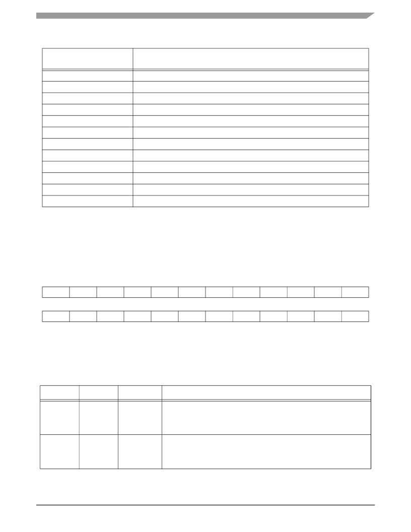
�PLL� Control� Register� (PCTL)�
�Table� 4-6.� Interrupt� Source� Priorities� Within� an� IPL� (Continued)�
�Priority�
�Lowest�
�SCI� receive� data�
�SCI� transmit� data�
�SCI� idle� line�
�SCI� timer�
�TIMER0� overflow� interrupt�
�TIMER0� compare� interrupt�
�TIMER1� overflow� interrupt�
�TIMER1� compare� interrupt�
�TIMER2� overflow� interrupt�
�TIMER2� compare� interrupt�
�EFCOP� Data� Input� Buffer� Empty�
�EFCOP� Data� Output� Buffer� Full�
�Interrupt� Source�
�4.5� PLL� Control� Register� (PCTL)�
�The� bootstrap� program� must� initialize� the� system� Phase-Lock� Loop� (PLL)� circuit� by� configuring�
�the� PLL� Control� Register� (PCTL).� The� PCTL� is� an� X-I/O� mapped,� read/write� register� that� directs�
�the� on-chip� PLL� operation.� (See� Figure� 4-5� .)�
�23�
�PD3�
�11�
�MF11�
�22�
�PD2�
�10�
�MF10�
�21�
�PD1�
�9�
�MF9�
�20�
�PD0�
�8�
�MF8�
�19�
�COD�
�7�
�MF7�
�18�
�PEN�
�6�
�MF6�
�17�
�PSTP�
�5�
�MF5�
�16�
�XTLD�
�4�
�MF4�
�15�
�XTLR�
�3�
�MF3�
�14�
�DF2�
�2�
�MF2�
�13�
�DF1�
�1�
�MF1�
�12�
�DF0�
�0�
�MF0�
�Figure� 4-5.� PLL� Control� Register� (PCTL)�
�Table� 4-7� defines� the� DSP56311� PCTL� bits.� Changing� the� following� bits� may� cause� the� PLL� to�
�lose� lock� and� re-lock� according� to� the� new� value:� PD[3–0],� PEN,� XTLR,� and� MF.�
�Table� 4-7.� PLL� Control� Register� (PCTL)� Bit� Definitions�
�Bit� Number�
�23–20�
�Bit� Name�
�PD[3–0]�
�Reset� Value�
�0�
�Predivider� Factor�
�Description�
�Define� the� predivision� factor� (PDF)� to� be� applied� to� the� PLL� input� frequency.�
�The� PD[3–0]� bits� are� cleared� during� DSP56311� hardware� reset,� which�
�corresponds� to� a� PDF� of� one.�
�19�
�COD�
�0�
�Clock� Output� Disable�
�Controls� the� output� buffer� of� the� clock� at� the� CLKOUT� pin.� When� COD� is� set,�
�the� CLKOUT� output� is� pulled� high.� When� COD� is� cleared,� the� CLKOUT� pin�
�provides� a� 50� percent� duty� cycle� clock.�
�DSP56311� User’s� Manual,� Rev.� 2�
�Freescale� Semiconductor�
�4-19�
�发布紧急采购,3分钟左右您将得到回复。
相关PDF资料
DSPAUDIOEVMMB1E
BOARD MOTHER DSP563XX
DSPIC30F2010 DEVELOPMENT KIT
KIT DEV EMBEDDED C
DSTRM-KT-0181A
DSTREAM DEBUG AND TRACE UNIT
DSUT1CSU
SURGE SUPPR NETWORK W/GROUND
DTEL2
SURGE SUPPRESSOR PHONE RJ11/RJ45
DV003001
PROGRAMMER PICSTART PLUS 16C/17C
DV164035
MPLAB ICD3 IN-CIRC DEBUGGER
DV164039
KIT DEV PIC24FJ256DA210
相关代理商/技术参数
DSP56311EVMIG_D
制造商:未知厂家 制造商全称:未知厂家 功能描述:DSP56311EVMIG DSP56311EVM Sample Code
DSP56311EVMUM
制造商:未知厂家 制造商全称:未知厂家 功能描述:DSP56311 Evaluation Module Hardware Reference Manual
DSP56311FACT
制造商:未知厂家 制造商全称:未知厂家 功能描述:DSP56311 Higher performance programmable DSP for demanding voice and data applications
DSP56311UM
制造商:未知厂家 制造商全称:未知厂家 功能描述:DSP56311 24-Bit Digital Signal Processor Users Manual
DSP56311UMAD
制造商:未知厂家 制造商全称:未知厂家 功能描述:DSP56311 Users Manual Addendum
DSP56311VF150
功能描述:数字信号处理器和控制器 - DSP, DSC 150Mhz/300MMACS 150Mhz EFCOP RoHS:否 制造商:Microchip Technology 核心:dsPIC 数据总线宽度:16 bit 程序存储器大小:16 KB 数据 RAM 大小:2 KB 最大时钟频率:40 MHz 可编程输入/输出端数量:35 定时器数量:3 设备每秒兆指令数:50 MIPs 工作电源电压:3.3 V 最大工作温度:+ 85 C 封装 / 箱体:TQFP-44 安装风格:SMD/SMT
DSP56311VF150B1
功能描述:数字信号处理器和控制器 - DSP, DSC 24 BIT DSP
RoHS:否 制造商:Microchip Technology 核心:dsPIC 数据总线宽度:16 bit 程序存储器大小:16 KB 数据 RAM 大小:2 KB 最大时钟频率:40 MHz 可编程输入/输出端数量:35 定时器数量:3 设备每秒兆指令数:50 MIPs 工作电源电压:3.3 V 最大工作温度:+ 85 C 封装 / 箱体:TQFP-44 安装风格:SMD/SMT
DSP56311VF150R2
功能描述:数字信号处理器和控制器 - DSP, DSC 24 BIT DSP RoHS:否 制造商:Microchip Technology 核心:dsPIC 数据总线宽度:16 bit 程序存储器大小:16 KB 数据 RAM 大小:2 KB 最大时钟频率:40 MHz 可编程输入/输出端数量:35 定时器数量:3 设备每秒兆指令数:50 MIPs 工作电源电压:3.3 V 最大工作温度:+ 85 C 封装 / 箱体:TQFP-44 安装风格:SMD/SMT