- 您现在的位置:买卖IC网 > Sheet目录323 > DSP56311EVM (Freescale Semiconductor)KIT EVALUATION FOR DSP56311
PLL Control Register (PCTL)
Table 4-6. Interrupt Source Priorities Within an IPL (Continued)
Priority
Lowest
SCI receive data
SCI transmit data
SCI idle line
SCI timer
TIMER0 overflow interrupt
TIMER0 compare interrupt
TIMER1 overflow interrupt
TIMER1 compare interrupt
TIMER2 overflow interrupt
TIMER2 compare interrupt
EFCOP Data Input Buffer Empty
EFCOP Data Output Buffer Full
Interrupt Source
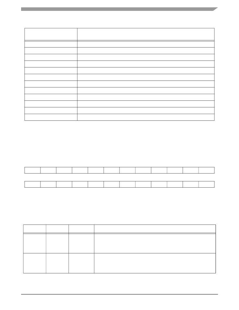
4.5 PLL Control Register (PCTL)
The bootstrap program must initialize the system Phase-Lock Loop (PLL) circuit by configuring
the PLL Control Register (PCTL). The PCTL is an X-I/O mapped, read/write register that directs
the on-chip PLL operation. (See Figure 4-5 .)
23
PD3
11
MF11
22
PD2
10
MF10
21
PD1
9
MF9
20
PD0
8
MF8
19
COD
7
MF7
18
PEN
6
MF6
17
PSTP
5
MF5
16
XTLD
4
MF4
15
XTLR
3
MF3
14
DF2
2
MF2
13
DF1
1
MF1
12
DF0
0
MF0
Figure 4-5. PLL Control Register (PCTL)
lose lock and re-lock according to the new value: PD[3–0], PEN, XTLR, and MF.
Table 4-7. PLL Control Register (PCTL) Bit Definitions
Bit Number
23–20
Bit Name
PD[3–0]
Reset Value
0
Predivider Factor
Description
Define the predivision factor (PDF) to be applied to the PLL input frequency.
The PD[3–0] bits are cleared during DSP56311 hardware reset, which
corresponds to a PDF of one.
19
COD
0
Clock Output Disable
Controls the output buffer of the clock at the CLKOUT pin. When COD is set,
the CLKOUT output is pulled high. When COD is cleared, the CLKOUT pin
provides a 50 percent duty cycle clock.
DSP56311 User’s Manual, Rev. 2
Freescale Semiconductor
4-19
发布紧急采购,3分钟左右您将得到回复。
相关PDF资料
DSPAUDIOEVMMB1E
BOARD MOTHER DSP563XX
DSPIC30F2010 DEVELOPMENT KIT
KIT DEV EMBEDDED C
DSTRM-KT-0181A
DSTREAM DEBUG AND TRACE UNIT
DSUT1CSU
SURGE SUPPR NETWORK W/GROUND
DTEL2
SURGE SUPPRESSOR PHONE RJ11/RJ45
DV003001
PROGRAMMER PICSTART PLUS 16C/17C
DV164035
MPLAB ICD3 IN-CIRC DEBUGGER
DV164039
KIT DEV PIC24FJ256DA210
相关代理商/技术参数
DSP56311EVMIG_D
制造商:未知厂家 制造商全称:未知厂家 功能描述:DSP56311EVMIG DSP56311EVM Sample Code
DSP56311EVMUM
制造商:未知厂家 制造商全称:未知厂家 功能描述:DSP56311 Evaluation Module Hardware Reference Manual
DSP56311FACT
制造商:未知厂家 制造商全称:未知厂家 功能描述:DSP56311 Higher performance programmable DSP for demanding voice and data applications
DSP56311UM
制造商:未知厂家 制造商全称:未知厂家 功能描述:DSP56311 24-Bit Digital Signal Processor Users Manual
DSP56311UMAD
制造商:未知厂家 制造商全称:未知厂家 功能描述:DSP56311 Users Manual Addendum
DSP56311VF150
功能描述:数字信号处理器和控制器 - DSP, DSC 150Mhz/300MMACS 150Mhz EFCOP RoHS:否 制造商:Microchip Technology 核心:dsPIC 数据总线宽度:16 bit 程序存储器大小:16 KB 数据 RAM 大小:2 KB 最大时钟频率:40 MHz 可编程输入/输出端数量:35 定时器数量:3 设备每秒兆指令数:50 MIPs 工作电源电压:3.3 V 最大工作温度:+ 85 C 封装 / 箱体:TQFP-44 安装风格:SMD/SMT
DSP56311VF150B1
功能描述:数字信号处理器和控制器 - DSP, DSC 24 BIT DSP
RoHS:否 制造商:Microchip Technology 核心:dsPIC 数据总线宽度:16 bit 程序存储器大小:16 KB 数据 RAM 大小:2 KB 最大时钟频率:40 MHz 可编程输入/输出端数量:35 定时器数量:3 设备每秒兆指令数:50 MIPs 工作电源电压:3.3 V 最大工作温度:+ 85 C 封装 / 箱体:TQFP-44 安装风格:SMD/SMT
DSP56311VF150R2
功能描述:数字信号处理器和控制器 - DSP, DSC 24 BIT DSP RoHS:否 制造商:Microchip Technology 核心:dsPIC 数据总线宽度:16 bit 程序存储器大小:16 KB 数据 RAM 大小:2 KB 最大时钟频率:40 MHz 可编程输入/输出端数量:35 定时器数量:3 设备每秒兆指令数:50 MIPs 工作电源电压:3.3 V 最大工作温度:+ 85 C 封装 / 箱体:TQFP-44 安装风格:SMD/SMT
